Monday, February 20, 2017


Week 7

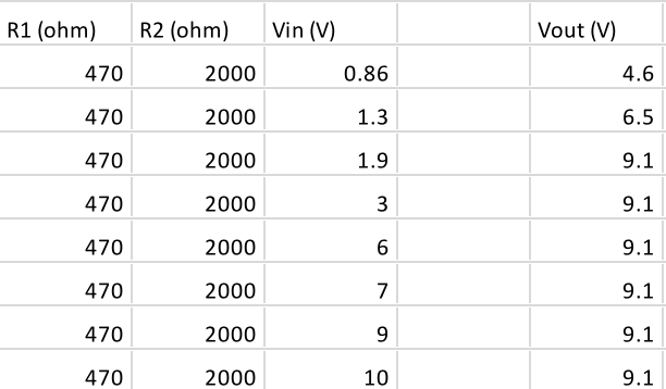
1. Force sensing resistor gives a resistance value with respect to the force that is applied on it. Try different loads (Pinching, squeezing with objects, etc.) and write down the resistance values. (EXPLAIN with TABLE)

Table 1.1 Various Force sensor resistance values.

Note in the table above that the resistance value at zero force is actually overlimit for the multimeter and not infinite. This only means that the resistance value is too high for the multimeter to read.

2. 7 Segment display:

a. Check the manual of 7 segment display. Pdf document’s page 5 (or in the document page 4) circuit B is the one we have. Connect pin 3 or pin 14 to 5 V. Connect a 330 Ω resistor to pin 1. Other end of the resistor goes to ground. Which line lit up? Using package dimensions and function for B (page 4 in pdf), explain the operation of the 7 segment display by lighting up different segments. (EXPLAIN with VIDEO).

Video 2.1 Explanation of seven segment display operation

b. Using resistors for each segment, make the display show 0 and 5. (EXPLAIN with PHOTOs)


Figure 2.1 Seven segment display showing 0

Figure 2.1 Seven segment display showing 5


3. Display driver (7447). This integrated circuit (IC) is designed to drive 7 segment display through resistors. Check the data sheet. A, B, C, and D are binary inputs. Pins 9 through 15 are outputs that go to the display. Pin 8 is ground and pin 16 is 5 V.

a. By connecting inputs either 0 V or 5 V, check the output voltages of the driver. Explain how the inputs and outputs are related. Provide two different input combinations. (EXPLAIN with PHOTOs and TRUTH TABLE)
UPDATE! You cannot actually measure the output voltages directly (I challenge you to figure out why!). You need to connect an LED and a resistor. LED’s positive terminal will go to 5 V. Negative terminal will be connected to your outputs via a resistor. The circuit would look like below:


Figure 3.1 Using 7447 display driver combination to display 0 on seven segment display

Figure 3.2 Using 7447 display driver combination to display 2 on seven segment display

Figure 3.3 Truth table 7447 display driver possible combinations and corresponding output for 0 to 9

b. Connect the display driver to the 7 segment display. 330 Ω resistors need to be used between the display driver outputs and the display (a total of 7 resistors). Verify your question 3a outputs with those input combinations. (EXPLAIN with VIDEO)


Video 3.1 Showing operation of each segment of the seven segment display using the 7447 display driver


4. 555 Timer:

a. Construct the circuit in Fig. 14 of the 555 timer data sheet. VCC = 5V. No RL (no connection to pin 3). RA = 150 kΩ, RB = 300 kΩ, and C = 1 µF (smaller sized capacitor). 0.01 µF capacitor is somewhat larger in size. Observe your output voltage at pin 3 by oscilloscope. (Breadboard and Oscilloscope PHOTOs)


Figure 4.1 555 timer connections top left of breadboard


Figure 4.2 555 timer clock signal measured on the oscilloscope

b. Does your frequency and duty cycle match with the theoretical value? Explain your work. 
Yes the frequency and duty cycle seem to be close to the theoretical value. Actual Frequency= 1/T = 1/0.55 = 1.8 Hz. 
Actual Duty cycle= 60% on 40% off
Theoretical Frequency=1.44/C(Ra+Rb)=1/(1uF(150K+300K))=1.89 Hz
Theoretical Duty cycle=Rb/(Ra+2*Rb)=300K/(150K+2*300K)=.40 The on/off time was 60% on and 40% off according to what we measured and the signal completed 1.8 cycles every second.

c. Connect the force sensing resistor in series with RA. How can you make the circuit give an output? Can the frequency of the output be modified with the force sensing resistor? (Explain with VIDEO)


Video 4.1 Showing the force sensing resistor in series with Ra


The force sensing resistor in series with Ra does not change the frequency of the 555 timer's output. The frequency is determined by the capacitors.


5. Binary coded decimal (BCD) counter (74192). This circuit generates a 4-bit counter. With every clock change, output increases; 0000, 0001, 0010, …, 0111, 1000, 1001. But after 1001 (which is decimal 9), it goes back to 0000. That way, in decimal, it counts from 0 to 9. Outputs of 74192 are labelled as QA (Least significant bit), QB, QC, and QD (Most significant bit) in the data sheet (decimal counter, 74192). Use the following connections:
5 V: pins 4, 11, 16.
0 V (ground): pins 8, 14.
10 µF capacitor between 5 V and ground.

a. Connect your 555 timer output to pin 5 of 74192. Observe the input and each output on the oscilloscope. (EXPLAIN with VIDEO and TRUTH TABLE)


Video 5.1 Input and output combinations of 74192 readings on the oscilloscope


Table 5.1 Input and output combinations Truth table 74192 for values 0 to 9.

6. 7486 (XOR gate). Pin diagram of the circuit is given in the logic gates pin diagram pdf file. Ground pin is 7. Pin 14 will be connected to 5 V. There are 4 XOR gates. Pins are numbered. Connect a 330 Ω resistor at the output of one of the XOR gates.

a. Put an LED in series to the resistor. Negative end of the LED (shorter wire) should be connected to the ground. By choosing different input combinations (DC 0V and DC 5 V), prove XOR operation through LED. (EXPLAIN with VIDEO)


Video 6.1 Using LED to prove XOR gate operation with different input combinations

b. Connect XOR’s inputs to the BCD counters C and D outputs. Explain your observation. (EXPLAIN with VIDEO)


Video 6.2 XOR inputs coming from BCD counter C and D outputs, connected to an LED to show XOR output of 1 or 0

When XOR output is 1 (BCD counter outputs are the opposite) the LED lights up, and when the XOR output is 0 (BCD counter outputs are the same) the LED turns off.

c. For 6b, draw the following signals together: 555 timer (clock), A, B, C, and D outputs of 74192, and the XOR output. (EXPLAIN with VIDEO)


Video 6.3 Explanation of the clock signal and A,B,C,D, and XOR output in a drawing

7. Connect the entire circuit: Force sensing resistor triggers the 555 timer. 555 timer’s output is used as clock for the counter. Counter is then connected to the driver (Counter’s A, B, C, D to driver’s A, B, C, D). Driver is connected to the display through resistors. XOR gate is connected to the counter’s C and D inputs as well and an LED with a resistor is connected to the XOR output. Draw the circuit schematic. (VIDEO and PHOTO)


Video 7.1 Shows the operation of the 555 timer, pressure sensing resistor,LED, display driver, seven segment display and XOR gate working together to light up an LED and to count from 0 to 9


Note that our seven segment display has a burnt out segment (top left vertical segment) that was later verified by directly providing power and ground to the segment with no operation.


Figure 7.1 Drawing of entire circuit above showing important components of circuit

8. Using other logic gates provided (AND and OR), come up with a different LED lighting scheme. (EXPLAIN with VIDEO)


Video 8.1 Proves operation of AND gate and OR gate 


Monday, February 13, 2017

Blog Sheet Week 6


Operational Amplifiers 
1. You will use the OPAMP in “open-loop” configuration in this part, where input signals will be applied directly to the pins 2 and 3. 
a. Apply 0 V to the inverting input. Sweep the non-inverting input (Vin) from -5 V to 5 V with 1 V steps. Take more steps around 0 V (both positive and negative). Create a table for Vin and Vout. Plot the data (Vout vs Vin). Discuss your results. What would be the ideal plot?

When we applied the lowest possible voltage (Vin) we still achieved the maximum Vout. This was due to the fact that we connected the OPAMP in open loop configuration. The ideal Plot would look very much like a digital signal with -3.79 Vout with any negative Vin, and 3.79 Out with any positive Vin.


Table 1.1 Open loop OPAMP configuration input and output voltages non-inverting 


Graph 1.1 Open loop OPAMP configuration input and output voltages non-inverting 

b. Apply 0 V to the non-inverting input. Sweep the inverting input (Vin) from -5 V to 5 V with 1 V steps. Take more steps around 0 V (both positive and negative). Create a table for Vin and Vout. Plot the data (Vout vs Vin). Discuss your results. What would be the ideal plot? 


Table 1.2 Open loop configuration OPAMP input and output voltage inverting

Graph 1.2 Open loop configuration OPAMP input and output voltage inverting 

2. Create a non-inverting amplifier. (R2 = 2 kΩ, R1 = 1 kΩ). Sweep Vin from -5 V to 5 V with 1 V steps. Create a table for Vin and Vout. Plot the measured and calculated data together. 


Table 2.1 OPAMP gain of 3, input and output voltage non-inverting


Graph 2.1 OPAMP gain of 3, input and output voltage non-inverting

3. Create an inverting amplifier. (Rf = 2 kΩ, Rin = 1 kΩ). Sweep Vin from -5 V to 5 V with 1 V steps. Create a table for Vin and Vout. Plot the measured and calculated data together.


Table 3.1 OPAMP gain of 3, input and output voltage inverting


Graph 3.1 OPAMP gain of 3, input and output voltage inverting

4. Explain how an OPAMP works. How come is the gain of the OPAMP in the open loop configuration too high but inverting/non-inverting amplifier configurations provide such a small gain? 

The OPAMP takes a set voltage (say 5 volts) and also takes a variable input voltage (-5 to +5 volts) and outputs a voltage equal to the gain multiplied by the variable input voltage; also if set up as inverting amp, it can output a voltage with the opposite sign. So input of +5V would give output of -5V. The theoretical maximum amplitude is the set voltage (5 volts). But realistically is a little lower than the set voltage. In open loop configuration the gain is theoretically infinite, but really it is still very high around (10^5). In inverting/non-inverting configurations the gain is reduced with the use of resistors to reduce the voltage being fed back into the input.


schematic view is the bottom view! 

1. Connect your DC power supply to pin 2 and ground pin 5. Set your power supply to 0V. Switch your multimeter to measure the resistance mode; use your multimeter to measure the resistance between pin 4 and pin 1. Do the same measurement between pin 3 and pin 1. Explain your findings (EXPLAIN).

The resistance between pin 1 and 3 with 0 Volts at pin 2 resulted in almost no resistance (about .6 ohms). When connecting the multimeter to pin 4 and 1 with 0 volts at pin 2, we measured an "overlimit" reading, which means it was open and there was no connection. So the resting position of the relay is pin 1 and 3 are connecting and when the relay is switched pin 1 and 4 are connected.

2. Now sweep your DC power supply from 0V to 8V and back to 0V. What do you observe at the multimeter (resistance measurements similar to #1)? Did you hear a clicking sound? How many times? What is the “threshold voltage values” that cause the “switching?” (EXPLAIN with a VIDEO). 


Video 2.1 Showing the operation of the relay with varying voltages

We noticed there were two audible clicks from the relay, 1st one was around 3V and the second usually occured around 6- 6.5 volts.


3. How does the relay work? Apply a separate DC voltage of 5 V to pin 1. Check the voltage value of pin 3 and pin 4 (each with respect to ground) while switching the relay (EXPLAIN with a VIDEO). 


Video 3.1 Shows the relay output change the switching the relay

We noticed that the output of volts at pin 1 changed when the relay was "switched".


LED + Relay 


1. Connect positive end of the LED diode to the pin 3 of the relay and negative end to a 100 ohm resistor. Ground the other end of the resistor. Negative end of the diode will be the shorter wire. 

2. Apply 3 V to pin 1 

3. Turn LED on/off by switching the relay. Explain your results in the video. Draw the circuit schematic (VIDEO)


Video 3.1 Relay controlled LED switching on and off


Operational Amplifier (data sheet under Bb/week 6) 

1. Connect the power supplies to the op-amp (+10V and 0V). Show the operation of LM 124 operational amplifier in DC mode with a non-inverting amplifier configuration. Choose any opamp in the IC. Method: Use several R1 and R2 configurations and change your input voltage (voltages between 0 and 10V) and record your output voltage. (EXPLAIN with a TABLE)

We were able to change the gain on the OPAMP by changing the resistance value ratio of R2 to R1. In the first table we achieved a gain of 3 ( 2000/1000 + 1 = 3 ), and the second table a gain of 5 ( 2000/470 + 1 = about 5 ).


Table 1.1 OPAMP non-inverting Vin and Vout values gain of 3


Table 1.2 OPAMP non-inverting Vin and Vout values gain of 5

2. Use your temperature sensor as your input. Do you think you can generate enough voltage to trigger the relay? (EXPLAIN)

We assume we would be able to generate enough voltage to trigger the relay with a heat source (hair dryer). Our hypothesis was that increasing temperature of the temp sensor would decrease the resistance of the sensor allowing enough voltage to flow to the relay.

3. Design a system where LED light turns on when you heat up the temperature sensor. (CIRCUIT schematic and explanation in a VIDEO) 

We were not able to show the operation of the temperature sensor, but we hypothesize that the temperature sensor varies in resistance with a change in temperature. This would affect the Vin and Vout of the OPAMP which would energize or turn the relay off, turning the led on and off.

4. BONUS! Show the operation of the entire circuit. (VIDEO)


Monday, February 6, 2017

Blog sheet week 5
1.       Functional check: Oscilloscope manual page 5. Perform the functional check (photo).


figure 1.1: Shows the functional check of oscilloscope probe


We verified that the oscilloscope probe was functioning correctly here above.

2.       Perform manual probe compensation (Oscilloscope manual page 8) (Photo of overcompensation and proper compensation).


figure 2.1: Photo of proper compensation


figure 2.2: Photo of overcompensation


When manually compensating the oscilloscope probe we were able to properly compensate the probe and also show what it looks like when we overcompensate.

3.       What does probe attenuation (1x vs 10x) do (Oscilloscope manual page 9)?

     The probe attenuation affects the vertical scale of the signal. 1x limits the bandwidth of the oscilloscope to 7Mhz while the 10x setting allows the full bandwidth of the oscilloscope to be used.

4.       How do vertical and horizontal controls work? Why would you need it (Oscilloscope manual pages 34-35)?

The horizontal and vertical controls allows adjustments of the scale of time and voltage. There is a vertical knob for each channel and one knob to adjust the position horizontally. There is also a horizontal scale knob to adjust the time frame of the signal. If a signal had a very short period you may need to shorten the time frame horizontally to view the signal. 

5.       Generate a 1 kHz, 0.5 Vpp around a DC 1 V from the function generator (use the output connector). DO NOT USE oscilloscope probes for the function generator. There is a separate BNC cable for the function generator.
a.       Connect this to the oscilloscope and verify the input signal using the horizontal and vertical readings (photo).


figure 5.1:horizontal and vertical readings on oscilloscope


We can view the horizontal and vertical readings on the oscilloscope and make adjustments on the scaling as well.

b.       Figure out how to measure the signal properties using menu buttons on the scope.

We pushed the autoset button to track the signal. Then adjusted the vertical and horizontal settings to get a good view the of the signal. Also note that we adjusted our function generator to .4V pp.

6.       Connect function generator and oscilloscope probes switched (red to black, black to red). What happens? Why?

When hooking the probes backwards the voltage signal is very low because the signal connected to ground and the ground is connected the signal measuring connector.

7.       After calibrating the second probe, implement the voltage divider circuit below (UPDATE! V2 should be 0.5Vac and 2Vdc). Measure the following voltages using the Oscilloscope and comment on your results:

a.   Va and Vb at the same time (Photo)


figure 7.1: Measuring ac voltage with oscilloscope at Va and Vb at the same time

Note that our amplitude was 1Vac with 2Vdc offset in our measurements.
b.   Voltage across R4.

The voltage across R4 was about 73.6 mVac peak to peak with an rms value of 25.0 mVac. Note that our function generator was set to 1Vac with 2Vdc offset in our measurements. 

8.       For the same circuit above, measure Va and Vb using the handheld DMM both in AC and DC mode. What are your findings? Explain.

Measuring with the multimeter we achieved .480Vac and .2.71Vdc on Vb. On Va there was .480Vac and 2.71Vdc. The multimeter gives the correct voltage reading because it is not grounded like the oscilloscope. There should be equal AC and DC at each point because the resistors have equal resistance and they are in series.


9.       For the circuit below
a.       Calculate R so given voltage values are satisfied. Explain your work (video)


Video 9.1 Shows how to calculate R7 using voltage divider

We had to convert the 2 Vac pp to rms value first, which is about .71 V rms. Then we knew that R7 consumed the other 4.29 V rms. Since R7 consumed about six times as much voltage as R6, we calculated R7 to be about 6K ohms.

b.       Construct the circuit and measure the values with the DMM and oscilloscope (video). Hint: 1kΩ cannot be probed directly by the scope. But R6 and R7 are in series and it does not matter which one is connected to the function generator.


Video 9.2: measuring R6 and R7 values with the DMM and oscilloscope.

We are just verifying our calculations from the problem above using the DMM and oscilloscope.

10. Operational amplifier basics: Construct the following circuits using the pin diagram of the opamp. The half circle on top of the pin diagram corresponds to the notch on the integrated circuit (IC). Explanations of the pin numbers are below:
1: DO NOT USE
8: DO NOT USE
2: Negative input
7: +10V
3: Positive input
6: output
4: -10 V
5: DO NOT USE

a.       Inverting amplifier: Rin = 1kΩ, Rf = 5kΩ (do not forget -10 V and +10 V). Apply 1 Vpp @ 1kHz. Observe input and output at the same time. What happens if you slowly increase the input voltage up to 5 V? Explain your findings. (Video)


Video 10.1 Shows our connections of an inverting amplifier

When we slowly increased the voltage on the function generator, the V out of the amplifier was changed from a sine wave to a digital signal (dc voltage).

b.       Non-inverting amplifier: R1 = 1kΩ, R2 = 5kΩ (do not forget -10 V and +10 V). Apply 1 Vpp @ 1kHz. Observe input and output at the same time. What happens if you slowly increase the input voltage up to 5 V? Explain your findings. (Video)

Video 10.2 Shows the connections on non-inverting amplifier

When we increased the input voltage on the non-inverting amplifier, we did not get a change  from a sine wave to a digital signal on the output this time. We believe there was an error in the connections because our output had a digital signal regardless of increasing or decreasing the input voltage.